Skip to content
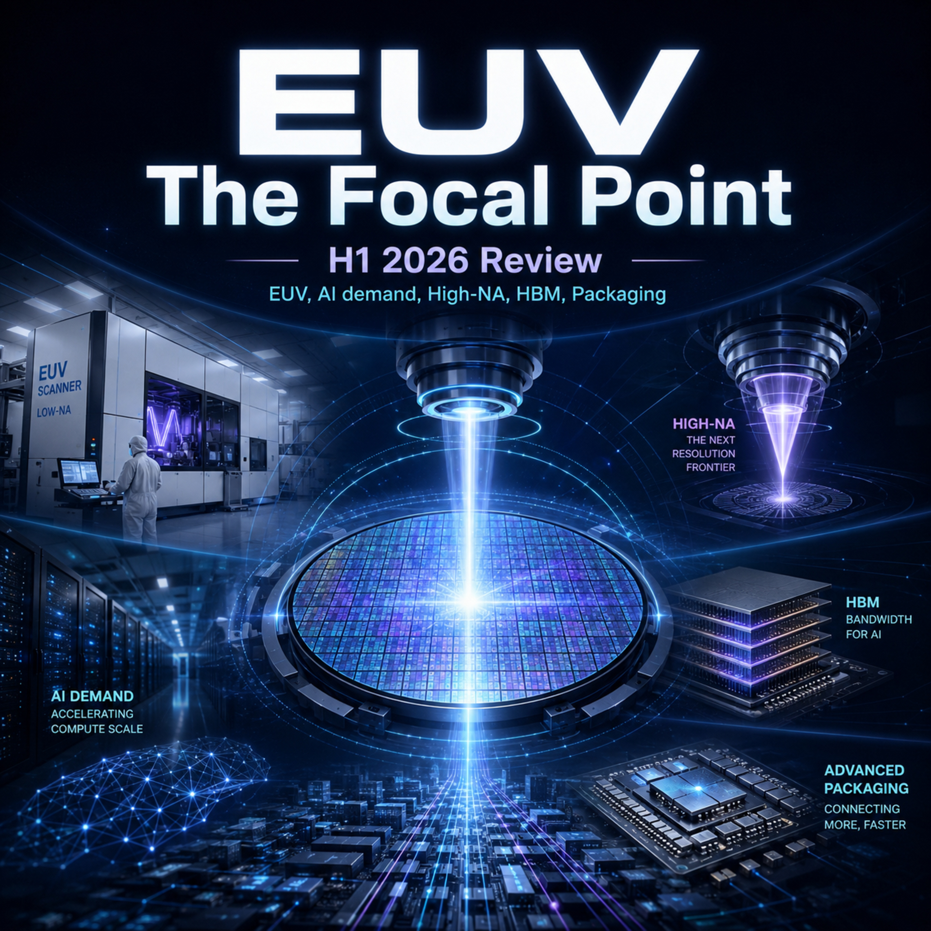
Artwork for EUV The Focal Point

EUV The Focal Point

EUV The Focal Point - Team

EUV The Focal Point is your Extreme Ultraviolet (EUV) lithography podcast.

Industry Briefings:
Cover leading-edge nodes, DRAM, HBM and strategy moves from ASML & co. and from the end customers Apple & co.

Focus Deep Dives:
Unpack physics, plasma, optics and how EUV scanners really work.

Hosted by EUV experts Samantha and Jack, built entirely with AI (a technology that itself relies on EUV-made chips ;-) using company newsrooms, Wikipedia and news sites.

AI can make mistakes: always verify the information independently before using it as a basis for business decisions.

Play
  • 28 episodes
  • weekly
  • Avg 16 min
  • English
Counted on this page — what you have heard stays on this device, so it is not something the list can be paged by.
  • S1 · E67
    Monday · 18 min

    [067] Industry briefing - EUV The Focal Point

    This post was created using AI. Please check the information if you want to use it as a basis for decision-making. New TSMC and Samsung figures reinforce the scale of semiconductor demand, while GlobalFoundries adds a dated interposer-supply plan for TSMC. The focus examines the Hyper-NA study's principal unresolved constraint: a smaller focus budget and the need for thinner resists. Architectural reuse could limit transition spending, but the proposed optics are not a commercial production commitment. Key takeaways - TSMC reported September revenue of NT$511.86 billion, up 54.6% year on year and down 0.6% month on month; January–September revenue grew 41.1%. - Samsung's preliminary Q3 guidance projects KRW195 trillion in consolidated sales and KRW107.4 trillion in operating profit, versus KRW12.17 trillion profit a year earlier; these are estimates, not final or foundry-specific results. - SIA reported sales exceeding US$1 trillion through August; its August figure of US$159.7 billion, up 8% sequentially, uses a WSTS three-month moving average. - Reuters reported AMD's plan for a substantial 2027 supply increase and need for more advanced wafer capacity; no wafer-volume, node-allocation or new-fab commitment was disclosed in those comments. - GlobalFoundries announced a US$2 billion agreement with TSMC for CoWoS silicon interposers, an initial five-year term and an expected Malta, New York volume ramp in H1 2028; this is packaging-component capacity. - The October 1 Hyper-NA paper proposes at least 0.75 numerical aperture at 13.5 nm and approximately 5 nm optical half-pitch; its roughly ten-year development estimate is not a committed delivery date. - The study identifies an approximately halved idealized depth of focus versus 0.55 NA, motivating better focus control and thinner resists; actual process windows remain pattern-dependent. - Source reuse leaves future power needs open; polarization can improve contrast but introduces a photon penalty, and a proposed 0.75-NA micro-exposure tool could support resist development. - ASML and TSMC have Q3 results scheduled for October 14 and 15 respectively; watch output guidance, advanced-node capacity and packaging execution, alongside measured Hyper-NA resist/focus results. Glossary EUV — Extreme ultraviolet lithography; the proposal retains the 13.5 nm wavelength. High-NA — High numerical aperture EUV; the 0.55-NA platform used as the study's comparison. Hyper-NA — Proposed EUV architecture with numerical aperture of at least 0.75. Half-pitch — Half the repeat distance of a periodic pattern; distinct from a commercial node name. Depth of focus — Axial imaging tolerance; an idealized optical value is not a complete manufacturing process window. Resist — Photosensitive patterning film; thinning it changes photon absorption and pattern-transfer requirements. Edge-placement error — Difference between an intended pattern edge and its realized position. Micro-exposure tool — Small-field research exposure system for developing materials under future optical conditions. CoWoS — Chip on Wafer on Substrate, TSMC's advanced packaging platform.
  • S1 · E66
    October 5 · 24 min

    [066] Industry briefing - EUV The Focal Point

    This post was created using AI. Please check the information if you want to use it as a basis for decision-making. Micron's September 30 results provide a concrete follow-up to last week's investment outlook, while Samsung projects a larger share of DRAM wafer capacity going to HBM. This episode examines how take-or-pay commitments improve investment visibility and why product mix, qualification and delivery timing still determine the EUV implications. Key takeaways - Micron reported fiscal Q4 2026 revenue of $54.23 billion and full-year net capital expenditure of $27.37 billion; financial growth is not a physical capacity measure. - Micron guides approximately $25 billion of net capex for the first half of fiscal 2027, with higher spending in the second half; $25 billion is not its full-year budget. - Samsung's Kim Taewoo expects HBM to use nearly 30% of industry DRAM wafer capacity in 2027, versus about 20% currently; this is an expectation, not market share or bit share. - Micron reports 26 multi-year take-or-pay SCAs, estimated to cover over 35% of revenue through 2030, with some agreements extending into 2031. - Micron identifies 1-gamma as its largest DRAM production node; its technology documentation confirms EUV use. - Micron says Singapore HBM packaging cleanroom preparation is ahead of plan, with initial output expected in early calendar 2027; packaging is distinct from front-end wafer capacity. - The September 28 outlook is partly answered on spending; a precise Micron HBM4E production date remains unestablished in the sources used here. - Analysis: translating contracted bits into exposure demand requires product mix, bits per wafer, yield and patterning-flow assumptions. - Fresh qualifying news was concentrated in memory; already-covered A14 pilot and silicon-wafer pricing reports were excluded from the news segment. Glossary EUV — Extreme ultraviolet lithography, used to pattern selected critical semiconductor layers. HBM — High Bandwidth Memory, a stacked DRAM product designed for high data bandwidth. DRAM — Dynamic Random-Access Memory, volatile memory used in computing systems. SCA — Strategic Customer Agreement; Micron uses this term for its multi-year customer supply arrangements. Take-or-pay — A contractual obligation to take an agreed quantity or make the required payment, subject to the agreement's terms. Net capex — Capital expenditure after the relevant offsets; Micron's guidance is net of anticipated government incentives. 1-gamma — Micron's EUV-enabled DRAM technology generation, also written 1γ. Front-end capacity — Wafer fabrication capacity, distinct from subsequent packaging and assembly. Qualification — Validation that a product or manufacturing process meets the relevant requirements before broader deployment.

  • S1 · E65
    September 28 · 13 min

    [065] Industry briefing - EUV The Focal Point

    This post was created using AI. Please check the information if you want to use it as a basis for decision-making. TSMC’s A14 program is becoming more operational: reported pilot timing is moving earlier while the design ecosystem is filling in with certified flows, interface IP and customer test-chip activity. At the same time, reported 300-millimeter wafer price pressure shows that AI-driven scarcity is moving deeper into the manufacturing supply chain. The EUV implication is important: more near-term pressure on the established EUV fleet does not mean TSMC is bringing High-NA production forward. Key takeaways - TrendForce reports that TSMC could begin A14 pilot production at Baoshan in 1Q27, while the company’s volume-production target remains 2028. - Cadence and Synopsys announced certified EDA flows for TSMC A14 at the 2026 North America OIP Ecosystem Forum. - Cadence says UCIe-64G IP has taped out on A14, adding a concrete interface-IP milestone to the node’s design ecosystem. - Analog Bits says its IP will be included in an upcoming customer test-chip tapeout on TSMC A14. - Siemens and TSMC are highlighting AI-assisted automated DRC fixing as a way to reduce manual design iterations and accelerate time to tapeout. - TrendForce reports that 2027 long-term agreement prices for 12-inch wafers could rise roughly 15–25% for epitaxial wafers and more than 40% for polished wafers. - The reported A14 pilot acceleration does not change TSMC’s recently stated 2030 start for High-NA EUV high-volume manufacturing. - No new ASML scanner shipment count was disclosed this week; the strongest EUV signals came from A14 readiness and upstream wafer supply. Glossary Extreme Ultraviolet (EUV) — Lithography using 13.5-nanometer light for the most demanding patterning layers in advanced logic and memory. High Numerical Aperture (High-NA) EUV — ASML’s next-generation EUV platform with higher numerical aperture for tighter single-exposure patterning. A14 — TSMC’s advanced logic process generation scheduled for volume production in 2028. Electronic Design Automation (EDA) — Software tools used to design, verify, implement and sign off integrated circuits. Design Rule Check (DRC) — Verification that a chip layout complies with foundry manufacturing rules. Tapeout — The point at which a chip design is finalized for mask generation and fabrication. Long-Term Agreement (LTA) — A multi-period commercial contract used to secure supply, pricing or both. 300-millimeter wafer — The standard silicon substrate diameter used for most advanced semiconductor manufacturing.

  • S1 · E64
    September 21 · 16 min

    [064] Industry briefing - EUV The Focal Point

    This post was created using AI. Please check the information if you want to use it as a basis for decision-making. ASML’s next EUV challenge is increasingly industrial rather than optical: reported 2028 capacity could exceed 110 systems, while the company appears committed to scaling its existing laser-produced-plasma source architecture rather than switching to free-electron lasers. At the same time, SK hynix is evaluating U.S. front-end manufacturing options, TSMC’s 2-nanometer node is gaining multiple flagship-mobile customers, and CXMT says its newest DRAM platform has entered mass production without EUV. Key takeaways - Reuters says ASML is examining ways to produce more than 110 EUV systems in 2028, with assembly speed reportedly the main constraint. - JPMorgan’s ASML readout says EUV intensity per chip is rising and High-NA adoption begins in 2028, becoming more meaningful over the following decade. - SiliconReport, citing JPMorgan, says ASML is unlikely to pursue a Free-Electron Laser source and is instead scaling laser-produced plasma toward roughly 1,000 watts. - SK hynix and Intel are discussing possible U.S. memory production involving Intel’s Ohio site, but SK hynix says no plan or partnership has been finalized. - Solidigm is separately considering a U.S. NAND factory, with upstate New York reported as a leading candidate; no investment decision has been made. - MediaTek’s Dimensity 9600 Pro uses TSMC’s 2-nanometer process, while Apple’s A20 Pro provides a second major flagship-mobile demand anchor for 2-nanometer production. - CXMT says its fifth-generation DRAM platform is in mass production using quadruple patterning, with 11.95-nanometer feature spacing and at least 50% more gross dies per wafer than its prior platform. - Micron and its Taiwan union completed a first mediation session without a reported production interruption; a second session is scheduled for October 22. - Unclear item: the product type, ownership structure, timing, and lithography requirements of any SK hynix-Intel U.S. memory project remain undisclosed. Glossary EUV — Extreme Ultraviolet lithography, the 13.5-nanometer exposure technology used for leading-edge semiconductor patterning. High-NA — High Numerical Aperture EUV, ASML’s higher-resolution EUV platform entering production selectively before broader adoption later in the decade. FEL — Free-Electron Laser, an accelerator-based light-source concept discussed as a possible alternative way to generate EUV radiation. DRAM — Dynamic Random-Access Memory, volatile working memory used in servers, PCs, smartphones, and accelerators. HBM — High Bandwidth Memory, stacked DRAM optimized for very high data throughput in AI and high-performance computing systems. NAND — Non-volatile flash memory used for persistent data storage. DUV — Deep Ultraviolet lithography, the established optical patterning platform that can be extended through multiple-patterning techniques. Gross dies per wafer — The theoretical number of dies patterned on a wafer before defective dies are removed from the count.

  • S1 · E63
    September 14 · 13 min

    [063] Industry briefing - EUV The Focal Point

    This post was created using AI. Please check the information if you want to use it as a basis for decision-making. High-NA EUV adoption now has clearer dates: TSMC says it intends to enter high-volume manufacturing in 2030, while Samsung targets advanced DRAM production in 2028. Intel’s new million-wafer disclosure and imec’s chemically amplified resist results show that the next phase is increasingly about reducing ecosystem cost and integration risk rather than proving the scanner can print. Key takeaways: - TSMC intends to use High-NA EUV in high-volume manufacturing for advanced nodes starting in 2030. - ASML and TSMC target a 12-inch photomask pilot line by 2031 and a path to advanced-node production readiness by 2033. - Samsung plans to introduce High-NA EUV into future DRAM high-volume manufacturing by 2028 and will join the 12-inch mask initiative. - Reuters reports that SK hynix also plans High-NA production from 2028, while Micron has ordered systems but has not disclosed a production date. - Intel Foundry and ASML say more than one million wafers have now been processed with High-NA across certification, R&D and selected Panther Lake volume-production layers. - Imec demonstrated CAR-based High-NA single patterning down to 22nm-pitch lines and 28nm center-to-center vias for logic-relevant structures. - The imec result suggests established chemically amplified resist technology can remain useful for several critical A14/A10-class layers, reducing early integration burden. - Samsung and SK hynix rejected a proposed 25 trillion won upfront payment to finance power infrastructure for planned Korean semiconductor mega-clusters, leaving an important capacity-enablement question unresolved. Glossary: Extreme Ultraviolet (EUV) lithography — Lithography using 13.5nm-wavelength light for advanced semiconductor patterning. High Numerical Aperture (High-NA) EUV — ASML’s next-generation EUV platform using higher numerical aperture for finer patterning. Chemically amplified resist (CAR) — A mature photoresist platform in which exposure triggers chemistry that amplifies the imaging reaction. High-volume manufacturing (HVM) — Stable, sustained production at commercial fab scale. Photomask — The patterned optical template used to transfer circuit features during lithography. Stitching — Combining adjacent exposure fields to create a pattern larger than a single High-NA exposure field. Dynamic Random-Access Memory (DRAM) — Volatile memory technology used in computing systems and High Bandwidth Memory products. NXE platform — ASML’s established 0.33 numerical-aperture EUV scanner family. A14/A10 — Advanced logic technology generations in imec’s roadmap associated with ångström-class scaling.

  • S1 · E62
    September 7 · 10 min

    [062] Industry briefing - EUV The Focal Point

    This post was created using AI. Please check the information if you want to use it as a basis for decision-making. TSMC says its estimated equipment requirement for 2026 has risen to about 1.9 times the level projected at the end of 2025, showing how quickly AI demand is propagating into fab investment. This week also brings fresh signals from ASML’s Japan support expansion, semiconductor-material capacity in Taiwan, Micron labor risk, and the continuing gap between China’s DUV and EUV capabilities. Key takeaways - TSMC says its estimated 2026 semiconductor-equipment requirement reached about 1.9 times its end-2025 baseline by July. - TSMC is simultaneously building 13 fabs in Taiwan and another five or six overseas, yet says it still cannot fully meet customer demand. - ASML Japan reportedly plans to grow from roughly 500 employees to around 700 by 2030 as it supports Rapidus and other Japanese customers. - ASML’s Hokkaido engineering presence supporting Rapidus has reportedly increased from 24 people to about 50. - Solvay plans to more than double ultra-pure hydrogen peroxide capacity in Taiwan from 35,000 to more than 70,000 tonnes per year by the end of 2026. - Micron unions representing about 10,000 workers in Taiwan are threatening strike action over bonuses; more than 80% backed strike action in an August survey. - ZEISS semiconductor chief Frank Rohmund said roughly 15 years is a reasonable assumption for China to develop cutting-edge EUV, while stressing that progress is difficult to measure externally. - UBS analysts reportedly estimate that Chinese immersion DUV systems could reach high-volume manufacturing within roughly two to five years. - Last week’s outlook on whether AI demand would translate into stronger upstream commitments now has a concrete TSMC datapoint: equipment requirements have nearly doubled versus the year-end planning baseline. Glossary Extreme Ultraviolet (EUV) — Lithography technology used for the most advanced logic and memory patterning. Deep Ultraviolet (DUV) — Earlier-generation optical lithography technology that remains essential across advanced and mature semiconductor manufacturing. High-volume manufacturing (HVM) — Stable, repeatable production at commercial wafer volumes rather than laboratory or pilot operation. Dynamic Random-Access Memory (DRAM) — Volatile memory technology used in servers, PCs, mobile devices, and High Bandwidth Memory stacks. High Bandwidth Memory (HBM) — Vertically stacked DRAM optimized for very high bandwidth in AI and high-performance computing systems. Fab — A semiconductor fabrication facility where wafers are processed. Field service — On-site installation, maintenance, repair, calibration, and operational support for semiconductor equipment. Ultra-pure hydrogen peroxide — High-purity process chemical widely used in semiconductor wafer cleaning. Equipment requirement — The quantity and mix of manufacturing tools a chipmaker estimates it needs to support planned wafer capacity.

  • S1 · E61
    September 3 · 23 min

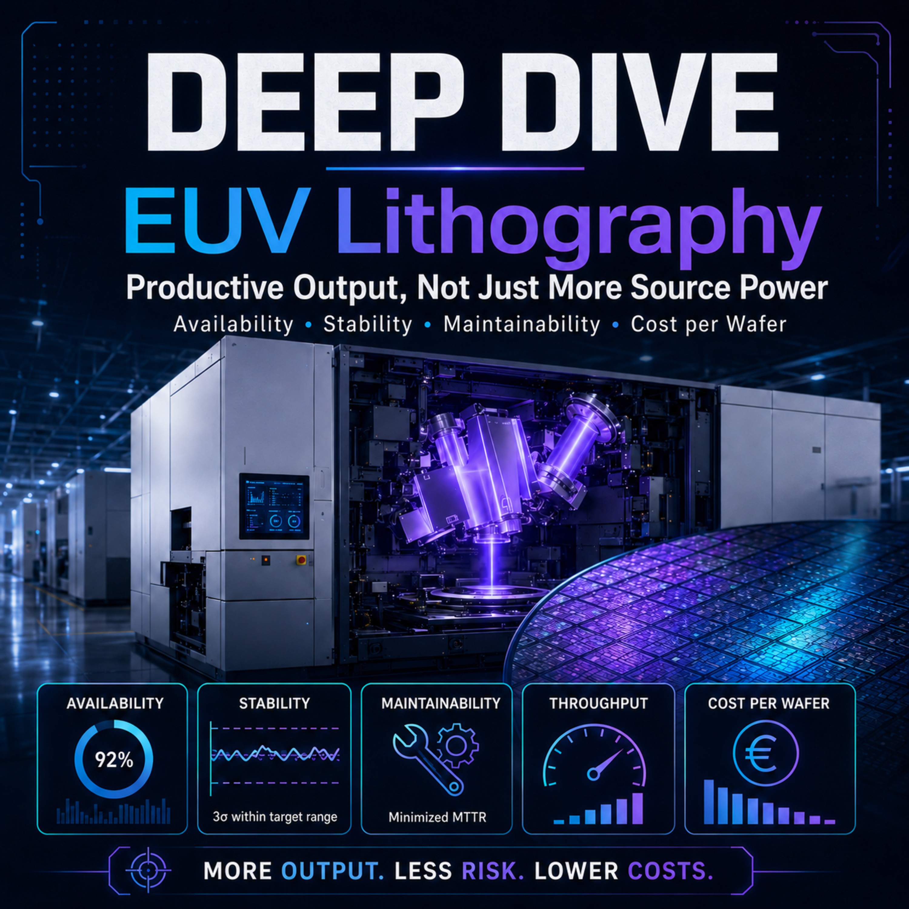
    [061] Deep Dive Topic - Beyond Watts: What Really Determines Productive EUV Output

    This post was created using AI. Please check the information if you want to use it as a basis for decision-making. Beyond Watts: What Really Determines Productive EUV Output EPISODE TEASER EUV lithography used to be dominated by one question: can the source generate enough 13.5-nanometer light for economical wafer throughput? In 2026, that is no longer the whole optimization problem. This episode explains why real fab value increasingly depends on productive output: throughput combined with availability, stability, maintainability, and cost per qualified wafer. KEY TAKEAWAYS - Source power remains a critical EUV enabler, but it is no longer a sufficient proxy for fab productivity. - Modern EUV throughput is a system property involving the source, wafer handling, precision stages, controls, metrology overhead, and process dose. - Nominal wafers per hour is condition-dependent; published low-NA throughput specifications are tied to a stated exposure dose. - Availability determines how often nominal scanner speed can actually be converted into fab capacity. - Power scaling must preserve source stability, collector lifetime, cleanliness, and serviceability to create production value. - Recent NXE:3800E gains came from a combination of higher source power, faster mechanics, improved handling, and software-based productivity upgrades. - Installed-base upgrades matter because fabs must extract more output from tools already in production, not only from newly purchased scanners. - The most useful economic endpoint is cost per qualified wafer, not maximum watts in isolation. - High-NA EUV reinforces the same lesson: imaging capability must mature together with throughput, availability, masks, resists, metrology, and service. GLOSSARY EUV lithography — Extreme ultraviolet lithography, a chip-patterning technology using light near 13.5 nanometers for leading-edge semiconductor manufacturing. Source power — The usable EUV optical power delivered by the light-source system; an important contributor to exposure speed. LPP — Laser-produced plasma, the EUV source method in which laser pulses strike tin droplets to create EUV-emitting plasma. Collector mirror — A multilayer mirror near the plasma source that gathers EUV radiation and directs it into the scanner. WPH — Wafers per hour, a scanner throughput metric measured under defined operating conditions. Availability — The share of scheduled production time during which a tool is capable of running production. Stability — The ability of the source and scanner to keep critical operating variables within the process window over time. Maintainability — How efficiently and predictably a system can be serviced and returned to production. Installed base — The population of lithography systems already operating at customer sites. Cost per wafer — The manufacturing cost allocated to each processed wafer, influenced by capital cost, throughput, uptime, service, energy, consumables, and yield-related performance.

  • S1 · E60
    August 31 · 5 min

    [060] Industry briefing - EUV The Focal Point

    This post was created using AI. Please check the information if you want to use it as a basis for decision-making. This week is light on new EUV scanner announcements but rich in semiconductor economics. NVIDIA’s demand, SK hynix’s U.S. HBM investment, Hot Chips memory disclosures, and Intel’s 18A-P versus possible TSMC sourcing choices show how utilization, wafer intensity, packaging, and capital allocation are becoming the decisive variables around advanced lithography. Key takeaways - NVIDIA reported Q2 FY2027 revenue of $96.2 billion and Data Center revenue of $89.0 billion, with Q3 revenue guided to $108.0 billion ±2%. - SK hynix broke ground on a more-than-$4-billion HBM packaging facility in Indiana; cleanroom opening is targeted for October 2028 and mass production for H2 2029. - The Indiana site will package and test advanced wafers made in South Korea, regionalizing the back end without duplicating the full EUV-intensive front-end flow in the U.S. - Micron said at Hot Chips that HBM requires roughly three times the wafer area of DDR5 for the same memory capacity, and that the ratio is not improving. - SK hynix indicated at Hot Chips that hybrid bonding is unlikely for HBM4E and may arrive with HBM5 at the earliest, extending the economic life of its current packaging approach. - Intel said Diamond Rapids uses Intel 18A-P, giving its leading-edge manufacturing platform additional internal volume. - TrendForce reported that Intel may consider TSMC N2X for some Razor Lake compute dies in 2027 depending on 18A-P performance; this remains unconfirmed. - Intel’s recent $20 billion equity offering and its Q2 Intel Foundry operating loss of about $2.1 billion underline why utilization and cost per good die matter as much as process milestones. - A useful follow-up to last week’s outlook arrived from SK hynix: a concrete capacity date is now available for Indiana, although not yet for the front-end M15X question. Glossary Extreme Ultraviolet (EUV) — Leading-edge lithography using 13.5-nanometer light for advanced logic and memory patterning. High Numerical Aperture (High-NA) EUV — ASML’s higher-resolution EUV platform used selectively by Intel in production learning. High Bandwidth Memory (HBM) — Stacked memory optimized for very high bandwidth in AI and high-performance computing systems. Dynamic Random-Access Memory (DRAM) — Volatile semiconductor memory; HBM is built from specialized DRAM dies. 18A-P — Intel’s performance-enhanced version of the Intel 18A process family. N2X — TSMC’s performance-oriented member of its 2-nanometer process family, targeted for 2027. Process Design Kit (PDK) — Foundry-provided design rules, models, and collateral used to build chips for a process. Hybrid bonding — Fine-pitch direct bonding approach intended to improve density and interconnect performance in advanced packages. Cost per good die — Manufacturing cost divided by the number of functional dies produced, combining yield, cycle time, and capital utilization.

  • S1 · E59
    August 27 · 16 min

    [059] Industry briefing - EUV The Focal Point

    This post was created using AI. Please check the information if you want to use it as a basis for decision-making. This week is less about a new EUV scanner milestone and more about the economics that determine when lithography capacity becomes valuable. Intel connects 18A-P to Diamond Rapids, Samsung and SMIC show renewed foundry pricing power, and Chinese memory investment continues to scale. Key takeaways: - Intel presented Diamond Rapids at Hot Chips 2026 and tied the product to Intel 18A-P and Foveros Direct 3D packaging. - The Hot Chips update partially answers an earlier podcast outlook asking whether Intel 18A-P risk production would become concrete product activity. - TrendForce reported that Intel may use TSMC N2X for some Razor Lake compute dies in 2027, but the sourcing plan remains unconfirmed. - Reuters reported Samsung raised prices for some new foundry orders by up to 15%, with its SF4 line at Pyeongtaek running at full capacity. - Samsung’s price increases are an indirect EUV signal because high utilization improves the economics of installed advanced-node lithography capacity. - SMIC reported second-quarter revenue above $3 billion, wafer shipments up 14% sequentially, average selling prices up 5.7%, and utilization at 93.7%. - YMTC’s parent plans a roughly RMB 33 billion Shanghai IPO to fund production upgrades and advanced-storage R&D. - The week’s central theme is manufacturing optionality: Intel can push 18A-P while preserving TSMC options, and customers are paying more to secure scarce capacity. - No major new official ASML EUV shipment or High-NA production milestone was identified for this week. Glossary: Extreme Ultraviolet (EUV) — 13.5-nanometer lithography used for the most demanding layers in advanced logic and memory manufacturing. Intel 18A-P — Intel’s performance-enhanced extension of the Intel 18A process family. N2X — TSMC’s high-performance extension of its 2-nanometer process family, targeted at performance-sensitive applications. Foundry — A semiconductor manufacturer that fabricates chips designed by external customers. Utilization — The share of available manufacturing capacity actively being used. Average selling price (ASP) — Average revenue received per unit sold, such as a processed wafer. Foveros Direct 3D — Intel’s advanced 3D packaging technology for direct die-to-die integration. High Bandwidth Memory (HBM) — Stacked DRAM designed for very high bandwidth in AI and high-performance-computing systems. Deep Ultraviolet (DUV) — Older lithography technology still used across many semiconductor layers and in advanced production where EUV is unavailable or uneconomic.

  • S1 · E58
    August 18 · 14 min

    [058] Industry briefing - EUV The Focal Point

    This post was created using AI. Please check the information if you want to use it as a basis for decision-making. Samsung’s revised foundry roadmap puts High-NA EUV around the 1-nanometer-class generation in 2030 while extending the life of its Low-NA EUV platform. At the same time, record equipment spending, new equity financing, and packaging investments show that the economic race is increasingly about sequencing capital across the whole manufacturing system rather than adopting one tool first. Key takeaways - Samsung reportedly moved SF1.4 from a 2027 target to 2029 and plans High-NA EUV insertion with its 1-nanometer-class process around 2030. - Samsung’s roadmap implies continued Low-NA EUV use for SF1.4+ while the company concentrates near-term resources on the SF2 family. - Applied Materials reported record fiscal Q3 2026 revenue of $9.12 billion, up 25% year over year, and guided fiscal Q4 revenue to about $10.25 billion, plus or minus $500 million. - Applied Materials raised its calendar-2026 advanced-packaging growth expectation to more than 70%, reinforcing the broader process-equipment signal highlighted in the August 4 outlook. - Intel upsized its common-stock offering from $15 billion to $20 billion and expects approximately $19.7 billion of net proceeds; the company says proceeds may include capital expenditures and working capital. - TSMC approved about $29.44 billion of capital appropriations covering advanced technology, advanced packaging, specialty capacity, fabs, and facility systems. - TSMC and Sony signed a definitive agreement for a next-generation image-sensor joint venture in Kumamoto, with volume production targeted for 2029. - SPIL reportedly broke ground on a nearly NT$100 billion Douliu plant that will add CoWoS capacity, with first-phase operations planned for 2028. - Nanya Technology says it is evaluating potential expansion sites but has not made a decision on reported new fabs in Yunlin and Pingtung. - U.S. policy pressure is increasingly reaching foundries themselves, with lawmakers pushing stricter scrutiny of advanced-chip orders that could indirectly serve sanctioned Chinese firms. Glossary Extreme Ultraviolet (EUV) — Lithography using 13.5-nanometer light for critical patterning at advanced semiconductor nodes. High Numerical Aperture (High-NA) EUV — The newer EUV platform intended for tighter critical-layer patterning and selective future-node insertion. Low Numerical Aperture (Low-NA) EUV — The established 0.33-NA EUV platform used broadly in current advanced logic and memory production. SF2 — Samsung Foundry’s 2-nanometer-class process family. SF1.4 — Samsung Foundry’s 1.4-nanometer-class process generation, now reported for 2029. Intel 14A — Intel Foundry’s next-generation process platform planned after Intel 18A. CoWoS — Chip on Wafer on Substrate, an advanced packaging approach used for large AI accelerators and HBM integration. HBM — High Bandwidth Memory, stacked memory used with advanced AI and high-performance computing processors. DRAM — Dynamic Random-Access Memory, the volatile memory technology underlying mainstream memory products and HBM.

  • S1 · E57
    August 14 · 26 min

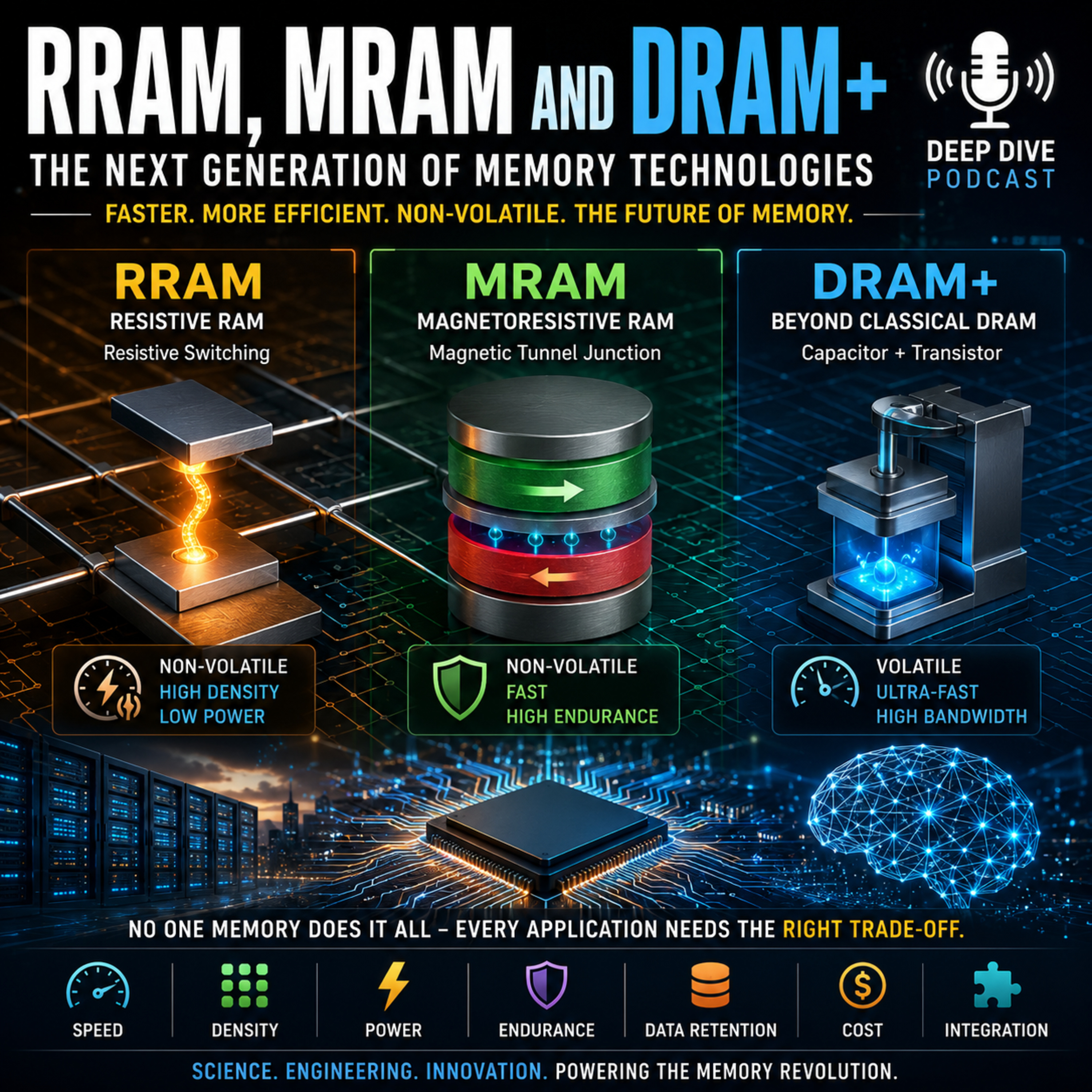
    [057] Deep Dive Topic - New Ways to Store Bits

    This post was created using AI. Please check the information if you want to use it as a basis for decision-making. EPISODE TEASER Why is the memory industry exploring RRAM, MRAM, and new DRAM concepts when SRAM, DRAM, and NAND already work so well? This episode explains the physical storage mechanisms, the engineering trade-offs, and the most realistic application paths. It also clarifies why “DRAM+” is an umbrella term rather than one standardized memory technology. KEY TAKEAWAYS - Every memory tier trades speed, density, energy, endurance, retention, cost, and integration complexity. - Conventional DRAM stores charge in a capacitor and must refresh it because the charge leaks away. - “DRAM+” can describe enhanced DRAM approaches such as HBM, gain-cell or capacitorless DRAM, three-dimensional integration, embedded DRAM, and processing near the memory. - RRAM stores information as resistance by moving ions or defects in a switching layer; variability is one of its central challenges. - STT-MRAM writes through a magnetic tunnel junction, while SOT-MRAM separates the read and write paths. - Nonvolatile memories reduce standby and refresh energy, but active write energy and peripheral circuits still matter. - RRAM and MRAM can support compute-in-memory, but array parasitics, data conversion, write control, and device variation limit idealized gains. - Advanced DRAM is the strongest near-term route for main memory; MRAM and RRAM are more likely to expand first in embedded and specialized roles. - The likely future is a more heterogeneous memory hierarchy, not one universal replacement. GLOSSARY DRAM — Dynamic random-access memory. Volatile memory that usually stores each bit as charge in a capacitor and requires periodic refresh. DRAM+ — A nonstandard umbrella term used here for enhanced DRAM cells, architectures, packaging, stacking, and processing-near-memory concepts. SRAM — Static random-access memory. Fast volatile memory commonly used for processor caches; a typical cell uses several transistors. NAND flash — Dense nonvolatile storage that retains data without power and is programmed and erased in larger groups than RAM. RRAM or ReRAM — Resistive random-access memory. Nonvolatile memory that stores data in different resistance states. MRAM — Magnetoresistive random-access memory. Nonvolatile memory that stores data in magnetic orientation and reads it through a resistance difference. STT-MRAM — Spin-transfer torque MRAM. A form of MRAM in which write current passes through the magnetic tunnel junction. SOT-MRAM — Spin-orbit torque MRAM. A form of MRAM with a separate lateral write path that acts on the magnetic free layer. Crossbar array — A grid of crossing conductors with a memory element at each intersection; useful for dense storage and parallel analog operations. Compute-in-memory — An architecture that performs selected operations in or very near memory arrays to reduce data movement.

  • S1 · E56
    August 10 · 11 min

    [056] Industry briefing - EUV The Focal Point

    This post was created using AI. Please check the information if you want to use it as a basis for decision-making. Nanya Technology has turned EUV memory expansion into a funded fab schedule, while TeraFab has gained a confirmed Texas site and an initial investment figure. AMD and TSMC provide fresh demand-side evidence, and reported Chinese-tool evaluations by Samsung and SK hynix show how export controls can reshape equipment qualification beyond lithography. Key takeaways - Nanya approved up to NT$346.6 billion of Fab 5A capital expenditure for 2026-2029, including EUV equipment. - Fab 5A is designed for 45,000 wafer starts per month, with first-phase capacity targeted at 35,900 WSPM. - Nanya plans wafer input in the second half of 2027, with 30,000 WSPM targeted for 2028 and 35,900 WSPM for 2029. - SpaceX and Tesla identified Grimes County, Texas, as the TeraFab site and announced an initial investment of $16.8 billion. - TeraFab still has no disclosed EUV scanner count, mask strategy, detailed process flow, or public production qualification schedule. - AMD reported Q2 2026 revenue of $11.5 billion; Data Center revenue was $6.7 billion, up 107% year over year. - TSMC reported July 2026 revenue of NT$467.58 billion, up 44.7% year over year. - Reuters reported evaluations of AMEC etch tools by Samsung and SK hynix, while both companies denied testing AMEC equipment for use in China and no broad deployment decision was reported. Glossary Extreme Ultraviolet (EUV) — Advanced lithography using 13.5-nanometer light for critical semiconductor patterning. Dynamic Random-Access Memory (DRAM) — Volatile memory used widely in servers, PCs, mobile devices, and AI systems. Wafer starts per month (WSPM) — A fab-capacity measure describing how many wafers enter production each month. 1C / 1D / 1E DRAM — Successive 10-nanometer-class DRAM process generations in Nanya’s roadmap. Capital expenditure (capex) — Spending on long-lived manufacturing assets such as fabs and production equipment. Etch — A semiconductor process that selectively removes material to transfer patterns into underlying layers. Mask strategy — The plan for photomasks and patterning steps used to manufacture a chip design. Process flow — The ordered sequence of fabrication steps used to build semiconductor devices.

  • S1 · E55
    August 6 · 9 min

    [055] Deep Dive Topic - Recap of H1 2026

    This post was created using AI. Please check the information if you want to use it as a basis for decision-making. In this H1 2026 review, EUV lithography is examined not as a single-machine breakthrough, but as the coordinating system behind AI-driven semiconductor manufacturing. The episode covers Low-NA productivity, the selective economic case for High-NA, rising HBM demand, advanced packaging, mask and metrology constraints, and the global expansion of leading-edge fabs. The central question is no longer who can print the smallest feature, but who can convert scarce tools, photons, engineering capacity, and cleanroom space into reliable compute at scale.

  • S1 · E54
    August 4 · 20 min

    [054] Industry briefing - EUV The Focal Point

    This post was created using AI. Please check the information if you want to use it as a basis for decision-making. This week’s episode looks beyond the EUV scanner to the design and manufacturing tools that turn advanced patterns into profitable silicon. SK hynix’s HBM4 ramp, strong results from Lam Research and KLA, and certified Synopsys flows for Intel 14A all point to the same conclusion: process integration and yield control are becoming as strategic as exposure capacity. Key takeaways - SK hynix reported second-quarter revenue of 79.3 trillion won and operating profit of 60.5 trillion won. - SK hynix began mass shipments of HBM4 in the second quarter and plans to ramp production in the second half of 2026. - SK hynix has finalized long-term agreements with around 10 customers and is accelerating the M15X mass-production schedule. - Lam Research reported record quarterly revenue of 6.72 billion dollars and guided the September quarter to about 8.1 billion dollars, plus or minus 400 million dollars. - KLA reported quarterly revenue of 3.66 billion dollars and guided the September quarter to 4.0 billion dollars, plus or minus 200 million dollars. - Synopsys certified AI-powered EDA and multiphysics flows for Intel 14A, including support across silicon, packaging, thermal, power-integrity, and electromagnetic analysis. - High-NA EUV economics depend on the full manufacturing flow, including masks, resists, etch transfer, metrology, design rules, and packaging. - Reuters reported that China has begun producing domestically developed immersion DUV lithography systems, although high-volume reliability and performance remain unproven. - No new official EUV scanner shipment count was identified this week; the strongest signals came from the surrounding equipment and design ecosystem. Glossary Extreme Ultraviolet (EUV) — Lithography using 13.5-nanometer light to pattern the most advanced semiconductor layers. High Numerical Aperture (High-NA) EUV — A higher-resolution EUV platform intended for selected critical layers at future advanced nodes. Deep Ultraviolet (DUV) — Lithography using longer-wavelength ultraviolet light; immersion DUV remains important across mature and advanced process flows. High Bandwidth Memory (HBM) — Vertically stacked memory designed to provide very high data bandwidth for AI and high-performance computing. Dynamic Random-Access Memory (DRAM) — Volatile working memory used in servers, computers, mobile devices, and HBM stacks. Electronic Design Automation (EDA) — Software used to design, verify, optimize, and prepare chips for manufacturing. Design Technology Co-Optimization (DTCO) — Joint optimization of chip design rules and process technology. Process control — Inspection, metrology, analytics, and feedback used to maintain yield and manufacturing stability. Multiphysics analysis — Combined modeling of electrical, thermal, mechanical, and electromagnetic effects in a chip and package.

  • S1 · E53
    July 30 · 23 min

    [053] Deep Dive Topic - Heterogeneous Integration: The Evolution of System Architecture

    This post was created using AI. Please check the information if you want to use it as a basis for decision-making. Heterogeneous integration is changing how advanced semiconductor systems gain performance. This episode explains why shrinking transistors is no longer enough on its own, how chiplets and advanced packaging connect specialized logic, memory, input-output, photonics, and other functions, and why artificial intelligence is accelerating the transition. It also examines the technical, economic, and supply-chain trade-offs behind the trend. KEY TAKEAWAYS - Transistor scaling remains essential, but modern performance gains increasingly come from system-level integration. - Heterogeneous integration combines dies made for different functions, process nodes, and sometimes different materials. - Chiplets can improve yield, reuse, product flexibility, and development speed. - Die-to-die links introduce latency, power, protocol, packaging, and test overhead. - Interposers, silicon bridges, through-silicon vias, and hybrid bonding enable dense communication inside advanced packages. - High-bandwidth memory is a central driver because artificial intelligence and high-performance computing are often limited by data movement. - Thermal management, mechanical stress, package warpage, and final assembly yield are major constraints. - UCIe aims to create a more interoperable chiplet ecosystem, but physical and manufacturing compatibility remain difficult. - Advanced packaging increases the strategic importance of foundries, assembly and test providers, materials, equipment, metrology, and design software. - Lithography remains critical both for leading-edge chiplets and for fine-patterned package structures. GLOSSARY Chiplet: A die designed to operate as one building block inside a larger multi-die system. Heterogeneous integration: Combining different dies, process technologies, functions, or materials in one package or system. Interposer: An intermediate wiring layer that provides dense connections between dies and the package substrate. High-bandwidth memory: Vertically stacked dynamic random-access memory designed for very wide, energy-efficient links to nearby processors. Through-silicon via: A vertical electrical connection passing through a silicon die or wafer. Hybrid bonding: Fine-pitch die or wafer bonding that joins copper connections and surrounding dielectric surfaces without conventional solder bumps. Two-and-a-half-dimensional integration: Side-by-side dies connected through a dense interposer or bridge. Three-dimensional integration: Active dies stacked vertically and connected with dense vertical links. Known good die: A die tested before assembly to reduce the risk of placing a defective component into an expensive package. UCIe: Universal Chiplet Interconnect Express, an industry specification for die-to-die communication.

  • S1 · E52
    July 27 · 19 min

    [052] Industry briefing - EUV The Focal Point

    This post was created using AI. Please check the information if you want to use it as a basis for decision-making. This week’s episode follows the shift from isolated chip orders toward integrated agreements covering logic, High Bandwidth Memory, packaging, optics, and data-center infrastructure. Samsung–Broadcom and NVIDIA–SK Group provide the demand signals, while ZEISS, Intel, and China’s memory makers show what the manufacturing system must deliver—and where its constraints remain. Key takeaways • Samsung and Broadcom signed an MOU estimated at more than $200 billion through 2030 across HBM, 2-nanometer-and-below foundry technology, and advanced packaging. • NVIDIA and SK Group announced a $500-billion-plus initiative that includes a 2-gigawatt AI factory and a long-term next-generation memory partnership. • SK Telecom plans the first facility in its NVIDIA Vera Rubin and SK hynix HBM4 buildout to come online in 2027. • ZEISS SMT is adding about 25,000 square meters of production and production-related space in Oberkochen, with High-NA EUV optics among the targeted technologies. • Reuters reported that planned CXMT fabs could lift capacity above 600,000 wafers per month, while restricted EUV access remains a major advanced-memory constraint. • CXMT shares rose 466 percent in their Shanghai debut after an $8.6 billion IPO. • Intel reported Q2 revenue of $16.1 billion; Intel Foundry revenue reached $5.8 billion, while the segment recorded an operating loss of about $2.1 billion. • No new industry-wide EUV scanner shipment total was disclosed this week; the demand signal is indirect and embedded in customer and supplier commitments. Glossary Extreme Ultraviolet (EUV) — Lithography using 13.5-nanometer light for critical layers in advanced logic and memory. High Numerical Aperture (High-NA) EUV — A newer EUV platform with higher optical resolution than conventional Low-NA EUV. High Bandwidth Memory (HBM) — Stacked dynamic random-access memory designed for very high data throughput near accelerators. Dynamic Random-Access Memory (DRAM) — Volatile working memory used in servers, personal computers, and many electronic systems. Deep Ultraviolet (DUV) — Mature lithography using longer wavelengths than EUV, often requiring more patterning steps at advanced dimensions. Memorandum of Understanding (MOU) — A framework describing intended cooperation that may precede binding commercial contracts. Risk production — An early manufacturing phase used to validate process maturity before broader volume production. Advanced packaging — Technologies that integrate multiple logic, memory, and interconnect components into one high-performance system.

  • S1 · E51
    July 21 · 11 min

    [051] Industry briefing - EUV The Focal Point

    This post was created using AI. Please check the information if you want to use it as a basis for decision-making. High-NA EUV infrastructure is moving from plans into physical installation as the first ASML EXE:5200 components reach Albany NanoTech. This episode examines why scanner power alone does not determine useful output: workforce retention, mask control, pellicle transmission, customer commitments, and research access increasingly shape EUV economics. Key takeaways - The first ASML TWINSCAN EXE:5200 components have begun arriving at Albany NanoTech, with first light targeted later in 2026 and research operations expected in early 2027. - Intel and Fortinet will collaborate on the Security Processor 6, but no process node, wafer volume, or EUV usage was disclosed. - ASML plans a €20,000 conditional retention grant for eligible employees who remain from 2027 through 2030. - Micron signed automotive Strategic Customer Agreements with seven major ecosystem partners to improve long-term supply, pricing, and technology visibility. - The 2026 EUVL and Source Workshop proceedings highlight rising mask-related variability, High-NA DRAM co-optimization, and higher-power EUV source development. - Lintec reports approximately 90% transmittance and up to 66-fold durability improvement for a carbon-nanotube pellicle under specified test conditions. - A 90%-transmitting pellicle leaves about 81% after two passes, while 95% leaves about 90%, illustrating why small transmission gains can materially affect dose and throughput. - This was a light week for new scanner shipment totals, and Intel’s manufacturing node for the Fortinet collaboration remains unclear. Glossary Extreme Ultraviolet (EUV) — Lithography using 13.5-nanometer light to pattern advanced semiconductor layers. High Numerical Aperture (High-NA) EUV — A higher-resolution EUV platform using 0.55 numerical aperture optics. Low Numerical Aperture (Low-NA) EUV — The established 0.33 numerical aperture EUV platform used in high-volume manufacturing. Pellicle — A thin membrane that protects a photomask from particles while transmitting exposure light. Reticle — The reflective EUV photomask carrying the circuit pattern projected onto a wafer. Dynamic Random-Access Memory (DRAM) — Volatile memory used in computing systems and as the base technology for high-bandwidth memory. Application-Specific Integrated Circuit (ASIC) — A chip designed for a defined function rather than general-purpose computing. First light — The first successful generation and operation of EUV light in an installed scanner.

  • July 16 · 19 min

    [050] Industry briefing - EUV The Focal Point

    This post was created using AI. Please check the information if you want to use it as a basis for decision-making. High-NA EUV has moved into a shipping logic product, with Intel and ASML qualifying selected Panther Lake layers on the EXE platform. ASML also raised its 2026 outlook and outlined major Low-NA and DUV capacity increases, showing that the next lithography era will be based on coexistence rather than immediate replacement. Key takeaways: - Intel Foundry is shipping a subset of Panther Lake products with selected Intel 18A layers dual-qualified on High-NA EUV. - ASML says yields on the High-NA-qualified layers match its established NXE Low-NA platform. - Intel is using High-NA selectively rather than replacing the full Intel 18A lithography flow. - ASML reported Q2 net sales of €9.3 billion, a 54.0% gross margin, and €2.9 billion net income. - ASML raised its 2026 sales outlook to €43–45 billion. - ASML plans to increase its approximately 65-system 2026 Low-NA EUV capacity by 30% for 2027. - SK Hynix completed a $26.5 billion U.S. ADR offering intended partly for fabs and equipment including EUV scanners. - Micron’s Hiroshima expansion targets equipment installation from the second half of 2028 and supports future EUV-enabled DRAM and HBM capacity. - High-NA adoption is likely to remain layer-selective until its cost-per-good-layer advantage is proven across more products. Glossary: Extreme Ultraviolet (EUV) — Lithography using 13.5-nanometer light for advanced semiconductor patterning. High Numerical Aperture (High-NA) EUV — ASML’s newer EUV platform with higher optical resolution than conventional EUV. Low-NA EUV — The established 0.33-NA EUV platform used in current high-volume logic and memory production. Intel 18A — Intel’s advanced process node used for Panther Lake processors. Dual qualification — Approval of two process or equipment routes to manufacture the same layer or product. NXE — ASML’s established Low-NA EUV scanner family. EXE — ASML’s High-NA EUV scanner family. American Depositary Receipt (ADR) — A U.S.-traded security representing shares in a foreign company. Dynamic Random-Access Memory (DRAM) — Volatile memory used as working memory in computing systems. High Bandwidth Memory (HBM) — Stacked DRAM optimized for very high data bandwidth in AI and high-performance computing.

  • S1 · E49
    July 6 · 14 min

    [049] Industry briefing - EUV The Focal Point

    This post was created using AI. Please check the information if you want to use it as a basis for decision-making. This week’s episode is a light week for new EUV scanner shipment numbers, but a strong week for capacity signals. South Korea moved from capital pledges to execution pressure, Samsung and TSMC showed how roadmap credibility now depends on design ecosystem readiness, and IBM’s nanostack work sharpened the question of what High-NA EUV must prove before production insertion. Key takeaways - No new official ASML EUV shipment count or High-NA production insertion milestone surfaced this week. - South Korea’s president pushed officials to accelerate chip and AI projects, emphasizing permits, land, power, and water as capacity bottlenecks. - Reuters reported expected investments of about 400 trillion won each from Samsung and SK hynix in southwest chip sites, plus 81 trillion won for a Chungcheong packaging cluster. - SK hynix’s Cheongju plan points to 100 trillion won of investment, including 80 trillion won for M17 NAND and 20 trillion won for P&T7 advanced packaging and test. - Samsung reaffirmed SF1.4 volume production for 2029 and SF1.4+ for 2030, while highlighting DTCO as a major contributor to SF2-to-SF2P gains. - Anthropic’s reported exploratory talks with Samsung on 2nm and advanced packaging remain unconfirmed but show AI companies seeking foundry optionality. - Socionext plans a September 2026 tape-out of a compute chiplet on TSMC A14, making A14 ecosystem readiness more concrete. - Nvidia’s China AI chip position is under pressure from Huawei and local suppliers, while China remains blocked from ASML EUV systems. - IBM’s nanostack announcement is research, not production, but it reinforces the value of early High-NA EUV learning at Albany. - Reported TSMC price increases, Apple product-cost pressure, and Broadcom’s Apple deal all point to scarcity being converted into pricing power and long-term contracts. Glossary Extreme Ultraviolet (EUV) — 13.5-nanometer lithography used for critical layers in leading-edge semiconductor manufacturing. High Numerical Aperture (High-NA) EUV — ASML’s next-generation EUV platform with higher resolution and a more demanding process ecosystem. Low Numerical Aperture (Low-NA) EUV — The current mainstream EUV platform used in high-volume manufacturing. Design Technology Co-Optimization (DTCO) — Joint optimization of chip design rules and manufacturing processes to improve power, performance, area, and yield. High Bandwidth Memory (HBM) — Stacked DRAM used beside AI accelerators to deliver very high memory bandwidth. Dynamic Random-Access Memory (DRAM) — Volatile memory used in servers, PCs, phones, and HBM stacks. NAND — Non-volatile flash memory used for storage in devices and data centers. Tape-out — The point when a chip design is finalized and sent for manufacturing masks and fab processing. Advanced packaging — Integration technologies that connect logic, memory, and chiplets into high-performance systems. Option value — The strategic value of learning early so companies can choose among technologies before production decisions are locked.

  • S1 · E48
    June 29 · 22 min

    [048] Industry briefing - EUV The Focal Point

    This post was created using AI. Please check the information if you want to use it as a basis for decision-making. This week’s episode looks at EUV as part of a broader manufacturing system rather than a standalone scanner story. South Korea’s cluster plans, Micron’s record quarter, SK Hynix’s proposed U.S. listing, Dutch pushback on export controls, ASML’s photonics work with TNO, and xLight’s light-source ambitions all point to the same theme: future lithography capacity is being financed and managed like strategic infrastructure. Key takeaways: - South Korea is preparing a new southwest semiconductor hub, with local reports suggesting investments could exceed 1,000 trillion won over several years. - The expected South Korean support package is infrastructure-heavy: power, water, land, workforce training, transport, and housing all matter for EUV-ready capacity. - Micron reported record fiscal Q3 revenue of $41.46 billion and said data-center revenue exceeded $25 billion in the quarter. - Micron has signed 16 strategic customer agreements and expects memory tightness to persist beyond calendar 2027. - Micron projects fiscal 2026 capex of about $27 billion and expects higher quarterly capex in fiscal 2027, with construction capex driving more than half the year-over-year increase. - SK Hynix plans to raise up to 45.45 trillion won, or about $29.4 billion, through a U.S. American Depositary Receipt listing. - Dutch officials are pushing back against the MATCH Act because it could force allies into U.S.-style China export controls and affect DUV servicing. - ASML and TNO will use DUV and I-line lithography in a new Eindhoven pilot line for six-inch indium phosphide photonic chips. - The xLight $350 million fundraising item remains reported rather than officially announced; the official anchor is the June 2 U.S. CHIPS Act award. - This week’s focus is a mixed-fleet view of lithography: EUV carries the densest layers, but DUV still carries much of scale, yield, reliability, and cost. Glossary: Extreme Ultraviolet (EUV) — Lithography using 13.5-nanometer light for the most critical layers in advanced logic and memory. High Numerical Aperture (High-NA) — Next-generation EUV optics with higher resolution potential, but higher cost and integration complexity. Deep Ultraviolet (DUV) — Lithography using longer wavelengths such as 193 nanometers and 248 nanometers, still essential for many advanced-node layers. Dynamic Random-Access Memory (DRAM) — Volatile memory used across servers, PCs, mobile devices, and high-bandwidth memory stacks. High Bandwidth Memory (HBM) — Stacked DRAM optimized for very high data bandwidth near AI accelerators and graphics processors. American Depositary Receipt (ADR) — A U.S.-traded certificate representing shares of a foreign company. Free-electron laser — A light source using accelerated electrons; xLight is developing this approach as an alternative EUV source. Indium phosphide (InP) — A compound semiconductor material used for active photonic functions such as lasers and modulators. Strategic customer agreement — A longer-term commercial agreement intended to improve supply visibility, pricing durability, or capacity commitment.

Showing 1–20 of 28 episodes